
flex-rigid and hdi pcb fabrication
Flex-rigid and high-density interconnect (HDI) PCB fabrication are two advanced manufacturing techniques that offer unique advantages and capabilities for electronic device design and assembly. Understanding the key differences between these two approaches is essential for selecting the most suitable option for specific applications and requirements.
Flex-rigid PCB fabrication involves the combination of flexible and rigid substrates within a single PCB design. This hybrid construction allows for bending and folding of the PCB while maintaining electrical connections between components and layers. Flex-rigid PCBs are well-suited for applications that require both flexibility and structural stability, such as wearable devices, automotive electronics, and aerospace systems.
On the other hand, hdi pcb fabrication focuses on achieving high-density interconnections and compact designs with multiple layers of traces and components. HDI PCBs use advanced manufacturing techniques such as laser drilling, sequential lamination, and microvia technology to create intricate and densely packed PCBs with precise control over critical parameters such as trace width, spacing, and impedance.
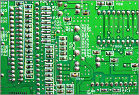
key differences between flex-rigid and hdi pcb fabrication
One key difference between flex-rigid and HDI PCB fabrication is the flexibility and bendability of the PCB. Flex-rigid PCBs are designed to bend and flex without compromising electrical connections or structural integrity, making them ideal for applications that require frequent bending or folding. In contrast, HDI PCBs are typically rigid and not designed to bend, although they can incorporate flexible substrates or flex-rigid constructions for specific applications.
Moreover, the complexity of the PCB design and assembly process differs between flex-rigid and HDI PCB fabrication. Flex-rigid PCBs require specialized design considerations and manufacturing techniques to accommodate the flexible and rigid portions of the board. This includes designing flexible sections with curved traces, staggered vias, and proper bending radiuses, as well as optimizing the assembly process to ensure reliable electrical connections between the flexible and rigid sections.
In contrast, HDI PCB fabrication focuses on achieving high-density interconnections and miniaturization through advanced manufacturing processes such as laser drilling, sequential lamination, and fine-line etching. This allows for the creation of PCBs with multiple layers of traces and components in a compact form factor, suitable for applications where space constraints are a primary consideration.
Another key difference between flex-rigid and HDI PCB fabrication is the cost and complexity of manufacturing. Flex-rigid PCB fabrication tends to be more complex and expensive due to the specialized materials, design considerations, and manufacturing processes involved in creating flexible and rigid sections within a single board. Additionally, flex-rigid PCBs may require custom tooling and assembly techniques, adding to the overall cost and complexity.
In contrast, HDI PCB fabrication can also be complex but offers advantages in terms of miniaturization, performance optimization, and cost-effectiveness. By leveraging advanced manufacturing techniques and materials, HDI PCBs can achieve high-density interconnections and compact designs without the need for flex-rigid constructions. This results in reduced manufacturing costs and simplified assembly processes compared to flex-rigid PCBs.
In conclusion, flex-rigid and HDI PCB fabrication offer distinct advantages and capabilities for electronic device design and assembly. Flex-rigid PCBs provide flexibility and structural stability, making them suitable for applications that require frequent bending or folding. HDI PCBs focus on achieving high-density interconnections and miniaturization, making them ideal for applications where space constraints, performance optimization, and cost-effectiveness are critical considerations. By understanding the key differences between these two approaches, designers and manufacturers can select the most suitable option for specific applications and requirements, ultimately leading to the development of innovative and reliable electronic devices.