
printed circuit board and assembly
Protecting electronic components and printed circuit boards (PCBs) from Electrostatic Discharge (ESD) is paramount during assembly and handling processes to prevent damage and ensure the reliability of electronic devices. ESD occurs when two objects with different electric potentials come into contact or close proximity, causing a sudden flow of electricity between them. The discharge of static electricity can result in voltages that exceed the tolerance levels of sensitive electronic components, leading to immediate or latent damage.
One of the primary methods for handling ESD during printed circuit board and assembly is to establish an Electrostatic Discharge Protected Area (EPA) or Electrostatic Protected Area (EPA) within the manufacturing facility. An EPA is a designated area equipped with ESD control measures, such as grounded workstations, ESD-safe flooring, and protective barriers, to minimize the risk of electrostatic discharge. Only personnel trained in ESD awareness and procedures are allowed to enter the EPA, and they must wear appropriate ESD protective equipment, such as wrist straps, heel grounders, and ESD smocks, to prevent the buildup and discharge of static electricity.
Additionally, all tools, equipment, and materials used in PCB assembly within the EPA must be ESD-safe and compliant with industry standards, such as ANSI/ESD S20.20 and IEC 61340. ESD-safe tools and equipment are designed to dissipate static charges and prevent the transfer of electrostatic energy to sensitive electronic components. This includes ESD-safe soldering irons, tweezers, trays, and packaging materials, as well as antistatic storage containers and packaging for components and PCBs.
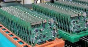
How do you handle ESD during printed circuit board and assembly?
Furthermore, proper grounding and bonding practices are essential for mitigating ESD risks during PCB assembly. All metallic surfaces, including workbenches, equipment, and fixtures, must be grounded to a common earth ground to equalize electric potentials and minimize the likelihood of electrostatic discharge. Bonding straps or cables should be used to connect grounded surfaces and personnel to the earth ground, ensuring continuous discharge of static electricity and preventing the buildup of electrostatic charges.
Moreover, handling and transporting electronic components and PCBs in ESD-safe packaging and containers is crucial for preventing ESD damage during assembly processes. Components should be stored and shipped in antistatic bags or containers with dissipative properties to shield them from external electrostatic fields and prevent electrostatic buildup. When handling components, workers should use grounded or ESD-safe gloves and avoid touching sensitive areas or pins to minimize the risk of ESD events.
During PCB assembly, ESD-sensitive components should be handled with extreme care to avoid damage from electrostatic discharge. Components should only be removed from their packaging and placed onto the PCB within the EPA, using ESD-safe tools and equipment. When inserting components into the PCB, workers should avoid excessive handling and ensure that components are properly aligned and seated to prevent damage from ESD events.
In conclusion, handling ESD during printed circuit board assembly is essential for protecting electronic components from damage and ensuring the reliability of electronic devices. By establishing Electrostatic Discharge Protected Areas (EPAs), using ESD-safe tools and equipment, implementing proper grounding and bonding practices, and handling components with care, manufacturers can mitigate the risks associated with electrostatic discharge and safeguard the integrity of PCB assembly processes. Compliance with industry standards and best practices for ESD control is critical for maintaining quality and reliability in electronic manufacturing operations.